Embedded Power Supply Control Card
Background
This project was taken while working on the Joint European Torus, the worlds largest nuclear fusion device. Creating fusion power requires a huge amount of energy and most of this is supplied by Neutral Beam Injectors. Neutral beams are created by accelerating positive Hydrogen ions towards a neutralising gas. The neutral particles then continue their path into the plasma, adding energy by collision. To get the particles to high enough speeds they are accelerated towards a grid (Grid 1) which is supplied by a high voltage power supply (~130kV).
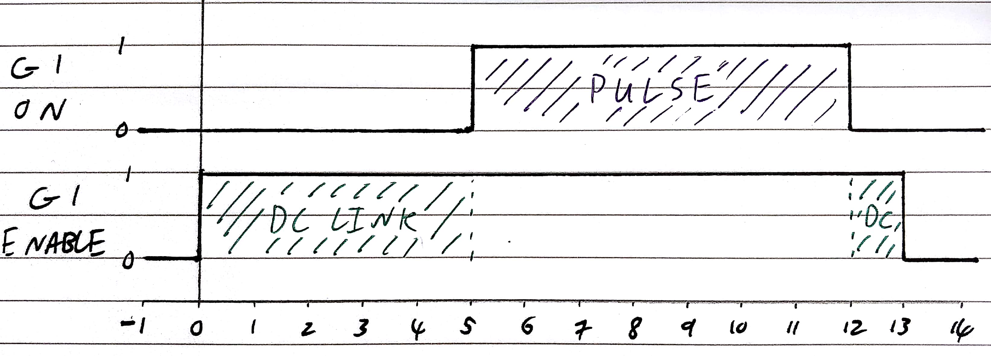
Grid 1 power supplies must be tested before operations by pulsing them onto a ‘dummy load’. The aim of this project was to design, test, and procure a PCB that would be installed into the supply and would carry out the dummy load test at the press of a button. This should be implemented using Fibre Optic transmitters and include a 5kHz safety signal that is constant. If the safety signal is lost or deviates in frequency then the supply will not pulse.
Due to the voltages involved the supply is also required to charge up a DC link before the full pulse and decharge it after. The output requirements are summarised as follows.
| Output | Description |
|---|---|
| G1 Enable | Enable DC link for 13 seconds |
| G1 On | Wait 5 seconds, then pulse supply for 7 seconds |
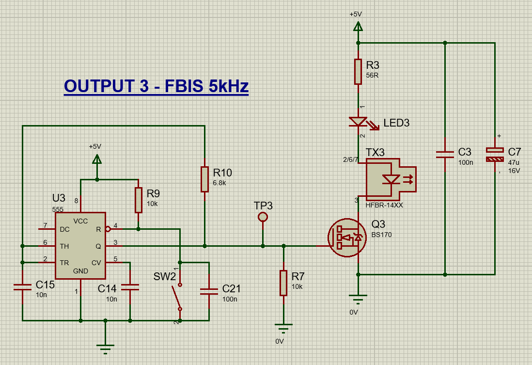
| FBIS | Constant 5kHz safety signal |
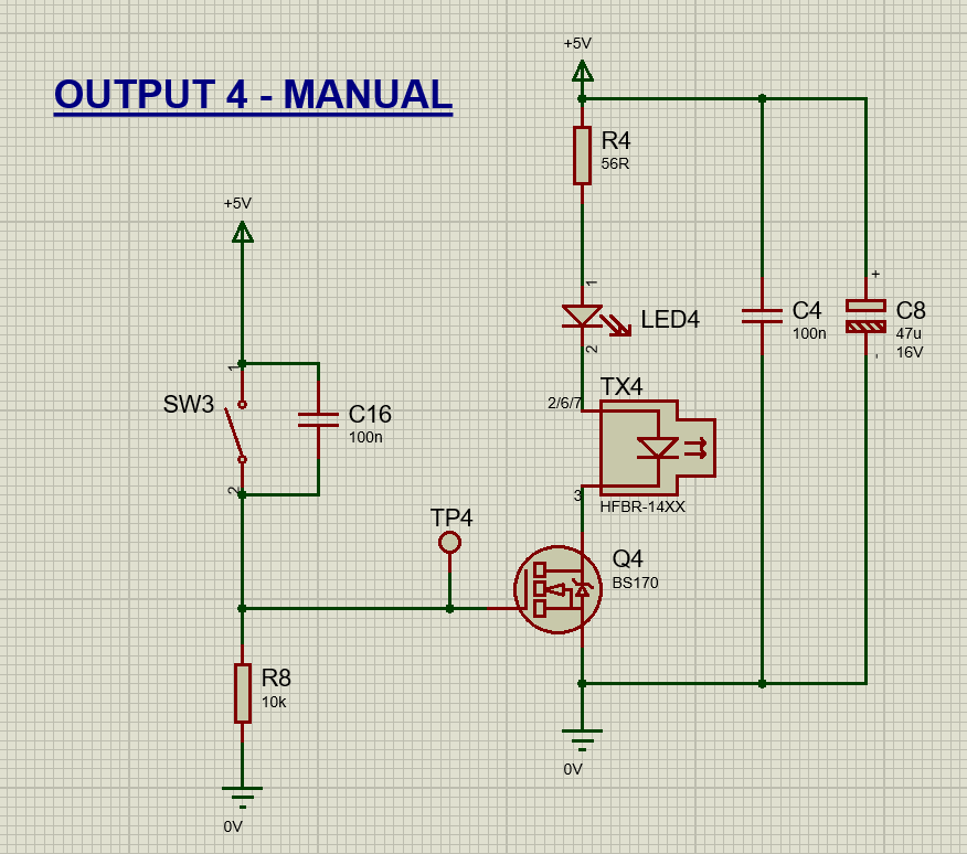
| Output 4 | Optional manual output |
The timing should look like this:
Design
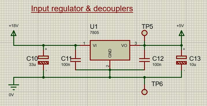
The cubicle that will host the card has an 18V supply rail that will be used to power the card. The first step is to convert from +18V to +5V using a voltage regulator and to smooth the input with decoupling capacitors.
The basic switched fibre transmitter is operated via a MOSFET (BS170) with a gate connected to the control source. There is also a status LED, two decoupling capacitors, and an input resistor to maintain correct current. The simplest set up is output 4, the manual switched output.
The other transmitters have the same peripheral hardware, each with a different control source connected to the MOSFET. For the safety signal this is an astable 555 timer, set up to output a constant 5kHz oscillation.
The control source for the main outputs, G1 Enable and G1 On, is an MCU (STM32F401RE). The MCU is connected to power through decoupling capacitors and is triggered by a push button. There are also various connections for USB and JTAG to enable flexibility in programming of the final product.
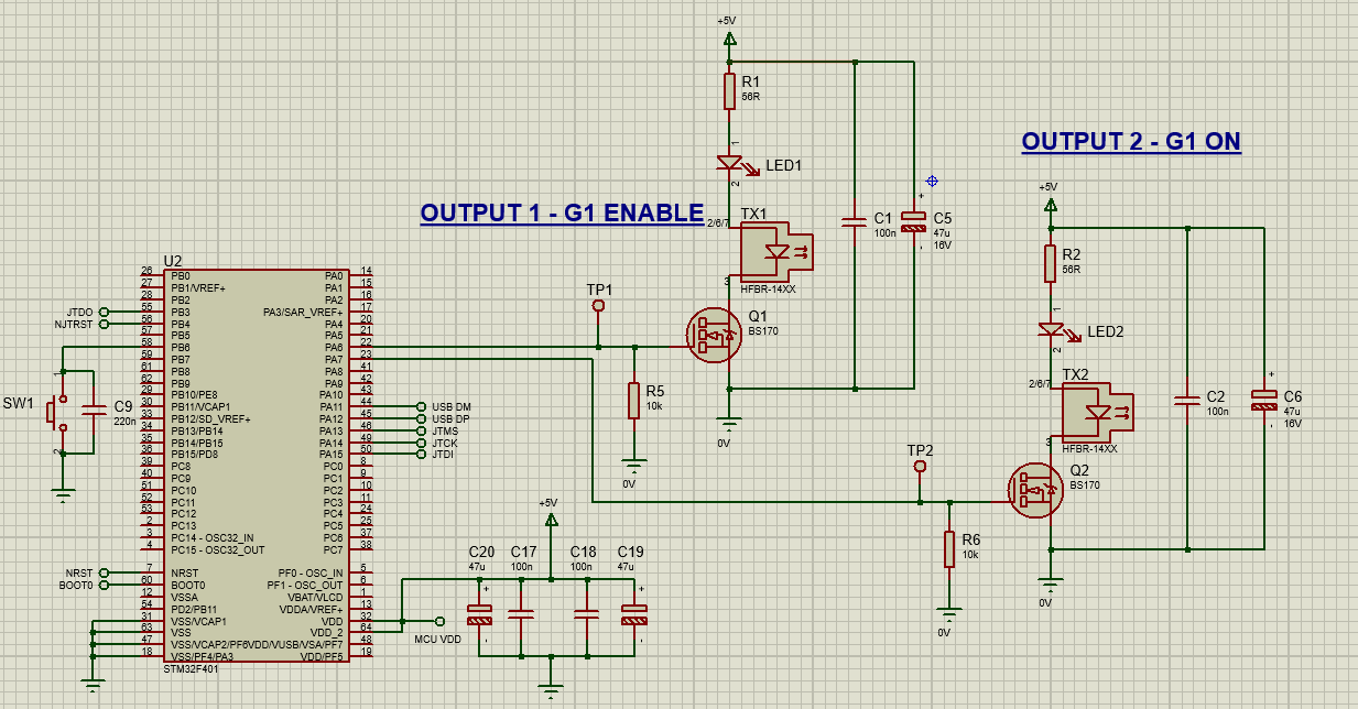
The code for the MCU was written in C++ using the ARM MBED environment.
#include "mbed.h"

// Declare pins
InterruptIn button(PB_6);
DigitalOut G1En (PA_6);
DigitalOut G1On (PA_7);

// Button function
void pressed()
{
    G1En = 1;
    wait(5.0);
    G1On = 1;
    wait(8.0);
    G1On = 0;
    wait(1.0);
    G1En = 0;
}

int main() {
    button.mode(PullUp);   // Set an internal pullup resistor for button
    button.fall(&pressed); // Trigger pressed function on falling edge
    while (1) {}           // Do nothing and wait for interrupt
}
This program is very simple, it takes the following actions in order:
- Define pins to use
- Define timing sequence for outputs
- Set internal pull-up resistor for button
- Run sequence when button pressed
- Wait for new press
Manufacture
Once the program was sufficiently tested on the development board (Nucleo-F401RE) a full prototype board was assembled.
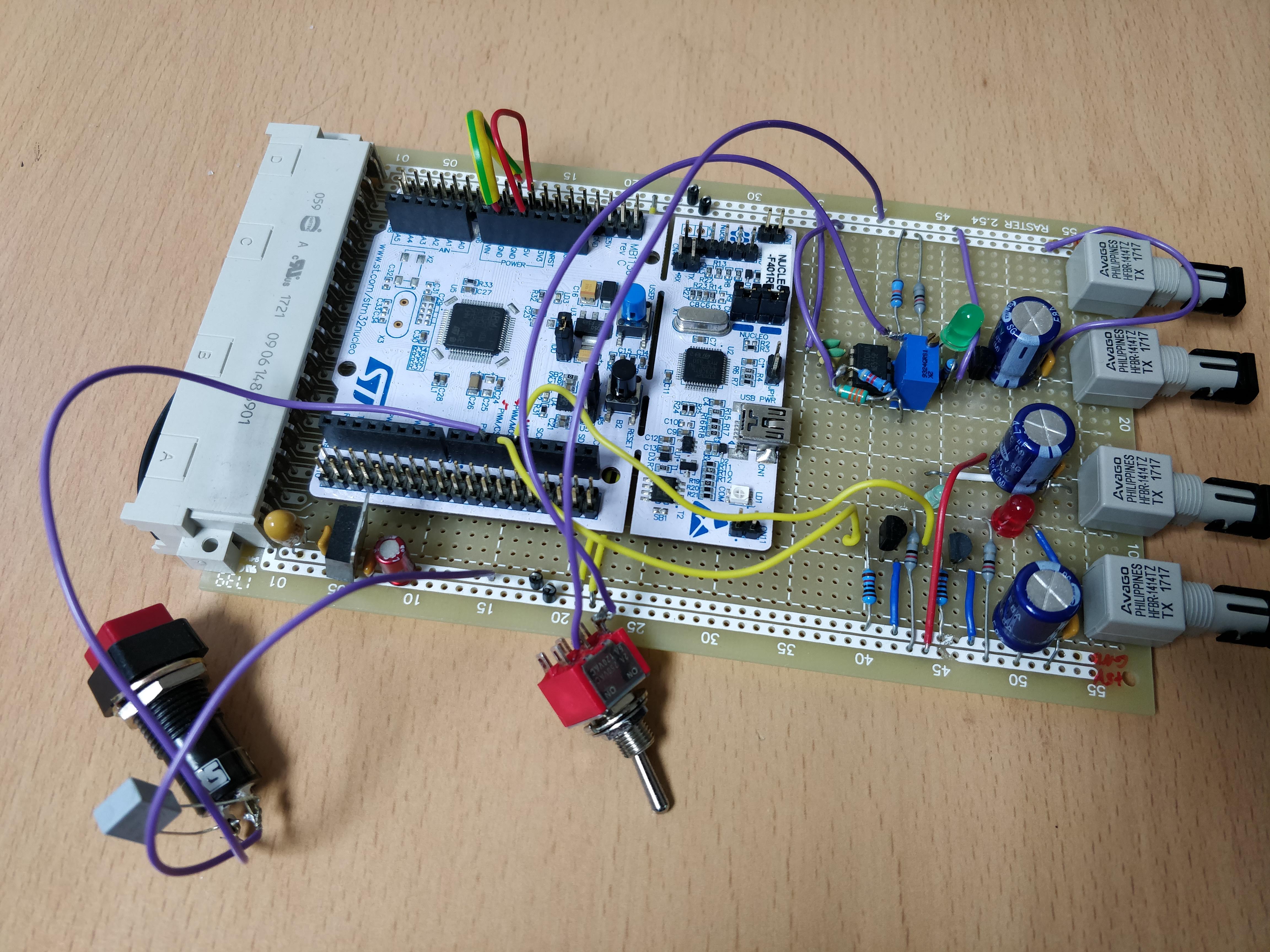
This was fully tested on the plant and operated as expected.
The design was then taken from schematic to PCB layout in Proteus. A two layer design with a single ground plane was used. A front panel for the board was also designed, insuring alignment with the fibre transmitters and screw holes.
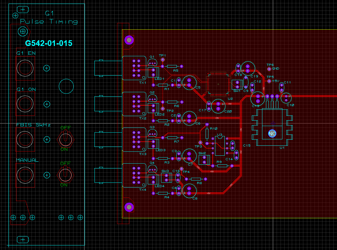
This design could be improved as there are some choke-points within the ground plane. A future revision may re-track the lines to more uniformly cover the top and bottom layers. Note: this design does not include programming/debugging terminals. The main power connector is off-screen to the right.
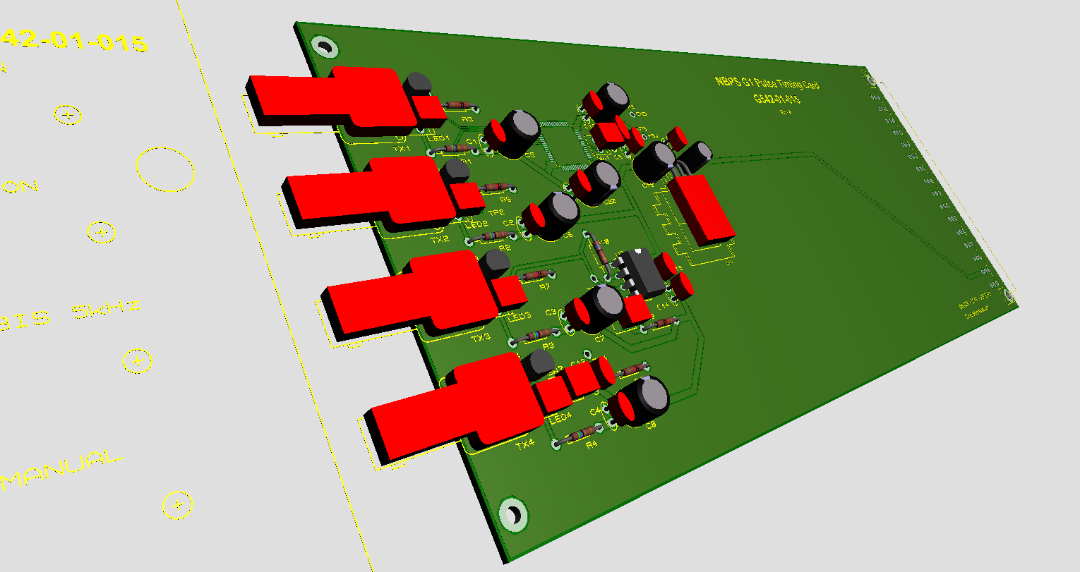
Proteus can also make a 3D visual to show how the final component will look.
The final stage of the process is generating a Bill of Materials (BOM) that specifies the components to be used on the final PCB. This involves searching component sites (RS, Mouser, Farnell), reading datasheets, and sometimes testing components in a lab. For example I tested the current consumption of the LED, Fibre Transmitter, and MOSFET in series to ensure the correct resistor value to use above them.
Proteus is used again to generate Gerber files which are sent, along with the BOM, to a manufacturer.